SOCL SMD High Power Amplifier with 2SC200 2SA1943
 |
| Parallel Transistor Final Amplifier |
In this post, Elcircuit will share the PCB Layout Parallel Final Transistor Amplifier file, this PCB serves to parallelize the final amplifier transistor, especially Class-AB where the goal is to parallel the final transistor so that the power generated by the power amplifier can be greater. for example, if you use a final transistor set with 2SC5200 and 2SA1943 final transistors and a power supply voltage of 80-90VDC CT, then a transistor set will only be able to load 8 ohms, if it gets smaller then the final transistor will be prone to damage.
.jpg) |
| 8 Ohm Load Amplifier OCL 90VDC CT |
because if the load is 4 ohms, the output current can reach 10A more, and this is not recommended for amplifiers that use 2SC5200 and 2SA1943 transistors if only one set, because the operation of the transistor is less safe.
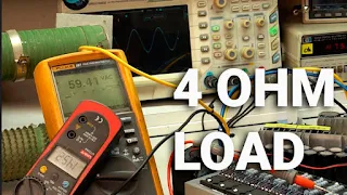 |
| Test Amplifier in 4 OHM Dummy Load Output Current up to 14.5A |
Then the solution can be added or paralleled with the final transistor. to parallelize the final transistors of class AB power amplifiers, it is quite easy to differ from class-D power amplifiers, a lot must be taken into account to add final transistors, so it's not as long as paralleling the final transistors for class-D power amplifiers. For Class-AB, if the final transistors are in parallel, the thing to note is the bias, the bias must be checked again, set B E about 300-600mV, if the bias is too high, the final transistor will be hot, if it is too small, the sound will be sluggish. and the bias is attempted to be balanced between + and - or 2SC5200 and 2SA1943 transistors.
Here's the Final Transistor Parallel PCB Layout
 |
| PCB Layout 2 Layer designed in EasyEDA |
The PCB above is designed with a dual-layer path, the final transistor is indeed made a bit tight so that the heat generated and transferred to the aluminum cooler will be more evenly distributed. For the use of the R Base, you can use 4R7-10R 1/4-1W Resistors and R Emitters use 0.22-0.56 Ohms because I'm paralleling the two resistors, I use a Watt resistor in the 2-3W range if 5W won't fit on the PCB.
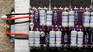 |
| Emitter Resistor using 0,47R 2W x2 each Transistor Final |
And you can download the PCB Layout at the end of the post, with the Gerber file format. then PCB Gerber can be printed on JLCPCB.
How to print PCB at JLCPCB can follow this step.
First, visit the JLCPCB site. then log in or register first (if you don't have an account) the button is in the top right corner. If you have logged into your account, then just click "Order Now"
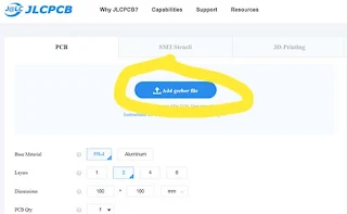
Then click "Add Gerber file"
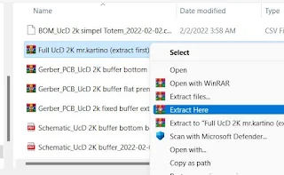
Select the Gerber file that has been downloaded at the end of the post link, but before using the downloaded file, the file with the name "Full UcD 2K mr.kartino (extract first)" must be extracted first.
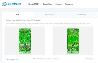
Then select Gerber one by one, then double click. Wait for the upload process to complete. then if you want to add another Gerber file, just click "Add Gerber file" again. if the three PCBs have been uploaded and you have selected the option for each PCB, click the basket, go to payment by clicking (Secure Checkout), and complete the payment on the next page. Payment can use a credit card, or debit visa, and also PayPal.
 |
| PCB Parallel Final Transistor printed on JLCPCB.com |
How to connect to the amplifier driver can be seen in the wiring diagram in the following figure.
 |
| Wiring with SOCL SMD Driver Amplifier |
The following is a description of the OCL power amplifier with 8 additional final transistors 2SC5200 and 2SA1943.
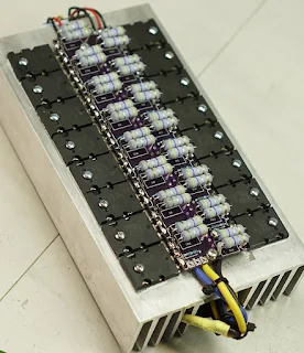 |
| 2SC5200 2SA1943 8 Set Final Transistors |
Super awesome
And the amplifier is strong if it is given a 90VDC CT power supply voltage and is given a load of 2 ohms, if it is 1 ohm it will be more stable.
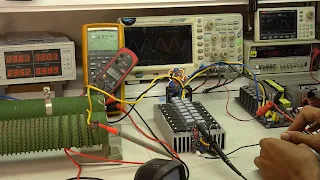 |
| 2 OHM Looad , Output Current Upto 28A. |
Video test
.jpg)
Post a Comment for "SOCL SMD High Power Amplifier with 2SC200 2SA1943"
Dont use outgoing links!