DIY Class-D Amplifier Fullbridge D2K 2500W RMS - Complete Build
Hello friends, in this post I will continue the D2K FB SMD project, which was Part1 ( Schematic, PCB, and BoM ) of the video yesterday about schematics, PCBs, and also how to order PCBs and SMD components that have been soldered.
In part 2 complete build, I will assemble, test the output power and sound of this power amplifier, troubleshoot and tips on optimizing this D2K power amplifier. I will post it in the next video, so the duration of the video is not too long.
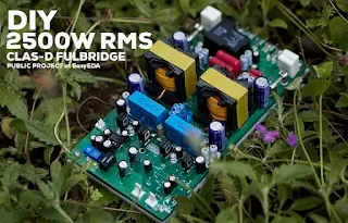
The following is the PCB, I design this PCB myself by using some SMD parts and DIP components.
Here are some SMD components that have not been soldered, I deliberately did not solder in JLCPCB. because I still have stock for the SMD component, so let me save more on the cost of soldering the SMD component.
First solder the SMD components that have not been filled. I use a mechanical brand Solder paste.
How to use it, apply enough on the PCB PAD to be soldered, so that the solder can be good try right at the PAD point. If applied evenly like this, the results can not be perfect. Usually, there is a solder combined. So it must be addressed again.
After that place, the SMD component, use tweezers to make it easier to take and put the SMD component. The SMD component is complete and ready to be soldered, I use a hot air solder to make soldering faster than using a soldering iron.
The hot temperature of the hot air solder I used was 300 degrees Celsius, with the least amount of air blowing. Use tools such as tweezers, to fix the location of SMD components that deviate or get off track.
Soldering is complete, and there are joined component legs. To fix, we can use a soldering iron by soldering directly pulled out. so that the joined tin can come loose, and don't forget to add more lead to the foot of the component that has not or is not soldered.
After all of the SMD components are soldered, install the DIP or Throughole components behind the SMD components, so the only ones visible above are the Throughole components.
To find out the location and component size values, you can directly open my project file, right away, by directly opening the D2K FB project, it will be easier for you to see in detail the component values, and you can also directly see the PCB path and the schematic. Visit the following link to open the D2K Fullbridge class-D project: EasyEDA Project Class-D D2K Fullbridge.
In the LPF capacitor section, I add a CAP 220N 250V in parallel to the outputs + and -. if you don't want to parallel, you can use 1.2uf capacitors on C31 and C32,
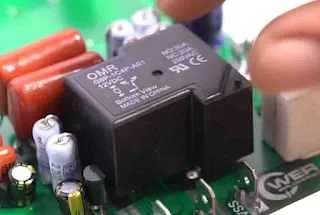
In the actual relay, there is a placement error, it should be located to the bottom layer, so it can be fitted if installed, the relay is actually slightly modified legs to fit into the relay hole. This does not affect the amplifier's performance.
For the LPF Inductor I use PQ35 cores that are given a custom gap, the gap is about 2mm. with an inductance value of 40uH, the two must as much as possible match the inductance value so that the power amplifier can work optimally.
For the MOSFET I use IRFP4242 93A 300V, besides the MOSFET you can also use the IRFP250 MOSFET, IRFP260, IRFP4227, 40N25, 76N25, IRFP4229. The required MOSFET is 4 seeds, 4 MOSFET seeds can handle thousands of watts.
The heatsink that I use is 10cm wide, 19cm long and 5mm thick, this is enough for this full-bridge amplifier, but a fan must be added, so that the air circulation is good. Although class-d has high efficiency, for power amplifiers with high power, it is better to have a fan, so that the performance is more stable.
Fullbridge Class-D amplifier is finished and ready to be tested, for testing, I use a switching power supply or SMPS, the symmetrical DC90VDC voltage. we first attach the main voltage cable Red to +, GND Blue, and black -.
The bias voltage is 12VDC + and - don't reverse, the PCB already has to mark for the +/- pin.
Then attach the Potentiometer to 10K ohms. and also input balance. for unbalance input, In - connects with gnd to gnd.
I will measure the AC output voltage without using the load first, and also see the output signal on the oscilloscope. and also PWM before passing the Low Pass Filter. I turn on the SMPS, the SMPS 90VDC output voltage is symmetrical.
The first start amplifier, the OCP led lights up, so to start it can be softer because when the OCP is active it will shut down the IR IC and also the speaker relay off, then the OCP will be off, PWM has started, can be marked by the dimming of the signal lights. (if the ripple is below 3Vpp) after that, the protection light is off and the speaker relay is on.
Input the 100Hz sine injection, add the volume, and the AC output voltage without load is around 110VAC. It has a maximum because I set the limiter, the output setting is the closest to the clip.
Next, I will install a 4ohm 1000W dummy load, along with its measurement tools.
let's test how much the output power. this input signal is still sine at 100Hz. we add volume slowly,
the maximum output voltage is 100.81VAC with a current of 25.10A so the output power of this amplifier is 2530,331W, we just round it up at 2500W RMS real output. : D Input sine 100Hz, load 4Ohm. With a 90VDC power supply voltage, so to maximize this amplifier it can supply 90VDC 30A per mono.
Next, I will test the sound, just small, using 18inch speakers.
In my opinion, the sound is very satisfying, even though it is focused on the use of subwoofer speakers, but the mid sound is clear, the clarity can be obtained. See the video make and test below.
Download Gerber File, BoM, Schematic PDF, CPL File for SMD Placement (SMT Assembly Service): 2500W RMS Class-D Amplifier SMD:
See part location on PCB, Schematic, BoM, and PCB Layout, : EasyEDA Project Class-D D2K Fullbridge
How to see a part number in PCB? You just open the link in EasyEDA Project and select PCB Layout, now you can see the PCB Layout and Part Number and Value on its, like this.
To see the number and value of the components:
1. Click the parts that you need to see.
2. See the table of components. Name: for value or name of components, and Prefix is the number in the schematic.
Tips:
See the see gate Mosfets signal, Use oscilloscope set the Time/Dive 500nS and V/div: 50V at high side and 10V at Low Side gate with the position in the top after that adjust position manually. Connect and probe to GND and + probe to gate MOSFETs.
 |
| Fig ( Scope 1) |
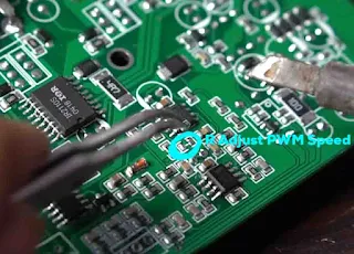
Fig (Scope 1) in the picture the oscilloscope displays the gate high and low side signals. And also display PWM Speed at 280kHz, the signal is still a little cross, I use IRFP4242 MOSFET, MOSFET is too heavy. to overcome this, I decrease the speed by replacing resistor R15 (1K see schematic), by reducing the value of the resistance, the PWM speed will go down. And if the resistance value increases, the PWM speed will rise. And also change resistor gate R31-R34 into 22R 1/4W resistor.
And here for the final result, the mini settings are amplifier settings that advertise youtube: Class-D 2500W RMS Fullbridge amplifier. PWM speed at 220 kHz, R adjust PWM at 560R, For LPF the inductor can be raised at 45uH and LPF cap 1.5 to GND each channel + and -. then 220n to the + and - channels.
And this the Ripple Output, Ripple output class D amplifiers with non-UcD topology should be around 3Vpeak to peak, don't over 4Vpeak to peak. and don't be less than 500mVpeak to peak. This greatly affects the quality and performance of class D.
How to measure it using an oscilloscope. use the GND Probe to + or - Output, and + Probe me + or - Output, warning if you are using a non-isolated probe, unplug all GND probe channels other than to measure output. Setting time / div at 500nS and Volt / div at 1V. What is measured is not the RMS value but the Peak to Peak Volt value.
This Project amplifier is FIXED and WORKING 100% (GUARANTEED) If you have difficulty assembling or there is a problem, please comment below. Recommended use SMT Assembly service to make it easier soldering SMD components.
.jpg)


Super class d amplifier, especially dimension and power are very good. Good job i want to make this.
ReplyDeleteyea you can make it, all files downloadable and its free. I can help if any problem, you can comment on this post.
DeleteThis super amplifier especially class-d amplifier has high power output
ReplyDeleteHie. I would like to make this amplifier. How much would it cost for the parts and I also didn't see the making of the power supply. Is that in a separate video?
ReplyDeleteThe powersupply not make by him, its product from indonesian
DeleteSr plz send garber file [email protected]
ReplyDeleteHi, can u help me? How many turns for the inductor? what the wire size diameter? i can use the t157-2? is same turns?
ReplyDeleteDiameter 4cm, no T157-2 use 40turns
DeleteDonde o como podría adquirir la tarjeta o PCB del amplificador
ReplyDeletehi,i like to ask can i use irfp460 to the board?
ReplyDeleteNot recomended
DeleteCan i use irfp460 mosfet to d2k5?
ReplyDeleteVery nice! If someone is interested in helping us build a quad-set of these PWM amplifiers to build a 3-phase test system, either as intern, by mentoring interns, or on project basis, please contact me at [email protected] for a proposal (we have a budget for this).
ReplyDeleteI am currently modifying Crown XLS2502 amps to build a test system for our solar inverter health scanner to improve the reliability of large renewable energy systems. As I don't get support from Crown/Harman, this is a much better starting point for increasing output current because our system measures a few hundred Amps. Reducing Amp-turns of our load to make up for lower output current of audio class-D amps would help increase system bandwidth due to lower inductance. Thanks!
Hi, how do you assure that there is enough deadtime between switching the mosfets? I dont see this as a feature of the mosfet driver you are using. Thanks very much in advance, Kind regards T
ReplyDelete