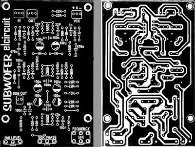
Subwoofer Filter NE5532 Schematic PCB
On this occasion, I will share the circuit for subwoofer filters in this subwoofer filter different from the previous filter or subwoofer module. In this circuit only use 3 pieces of Op-Amp IC which we usually encounter in tone control circuit, active crossover, a filter circuit, another preamp circuit that is IC NE5532. This IC is very popular so I will apply it to this filter subwoofer circuit and its circuit schematic.
In the above circuit, there are three settings for the subwoofer filter frequency, where the frequency can be filtered from 50Hz up to 300Hz. This frequency setting is on a 50K stereo with a FREQ label, then also there for subwoofer phase settings that we can use ranging from 0 to 180 degrees. Phase settings contained in Phase 100K pot. then the last is the level setting or also can be called the volume subwoofer, which is used to set the amount of voice signal to be transferred to a special power amplifier bass/subwoofer. Level settings contained in the 50K pot Level.
Buy NE5532 IC for this filter circuit from allchips.ai, see image and link below:
Buy NE5532 IC for this filter circuit from allchips.ai, see image and link below:
To facilitate the making of this filter subwoofer circuit I also share PCB Layout design below, with the size of PCB 107mm x 69mm.
DIY Subwoofer Filter Circuit
This Subwoofer Filter NE5532 is tested with Power Amplifier SOCL 504, see this video:
.jpg)


bagaimana mahu membeli kit ini tuan?
ReplyDeleteplease contact us me.
Deletefungsi pot phase utk apa ??
ReplyDeleteTo ask here as well since i didn't get any answer on YouTube video. What to change to make from 20hz to 150hz. Not from 50Hz up to 300Hz. I will appreciate you answer. Thanks
ReplyDeleteOkay you can modify thee circuit
ReplyDeleteOn B ic no audio signal output.its normal?I had try this schematic
ReplyDeletecan i use 4558 instead of 5532?
ReplyDeleteWhat are the 3 output pins next to input pins in top left corner?
ReplyDeleteWath is the voltage ratings of the capacitors? Do you have a BOM for the schematic? Pls
ReplyDeletethere a difference between the schematic and the pcb layout
ReplyDeleteWhere is the difference can u please tell me, I am planning to build it
DeleteBuilt the module as per schematic but it's not working... something is wrong in the schematic
ReplyDeleteis it working?, if working please provide me correct PCB layout and schematic on ([email protected]).
DeleteDear friend, I want to make this lowpass fielter, for my personel use.
ReplyDeletePlease send pdf or Gerber file to this email id ([email protected])
Thanks in advance
Dear friend, I want to make this lowpass fielter, for my personel use.
ReplyDeletePlease send pdf or Gerber file to this email id ([email protected])
Thanks in advance
Hi i want to now if you can send the PCB ? I want to make this circuit but don´t have a chance to make it. If you sell the circuit i can buy, even if it´s completed with all components.
ReplyDeleteBest regards
On schematic connections between pins 1 and 2 of IC-B and between pins 1 and 2 of IC-C (unity gain negative feedback in both cases) are missing. They are on PCB. Maybe there are other differences, but it seems to behave correctly now when simulated in LTSpice. T.
ReplyDeleteSchematic is wrong. It is missing short connection between pin 1 and 2 on chip B and also on chip C. On PCB it is OK. If you design your own PCB you should correct this.
ReplyDeleteThis is a best low pass filter
ReplyDelete