Power Amplifier 1000W Rocky TEF
Hello friends, this time I will share project about Power Amplifier with the name of Rocky TEF power amplifier with output power up to 1000 Watt RMS. With high power category, this amplifier is capable of controlling 12Inch speakers A total of 4 even 6 pieces with each speaker power of 300W. The following is a project of making this Rocky TEF power amplifier, starting from circuit scheme, PCB Layout, and also there is video assembly, also testing power amplifier.
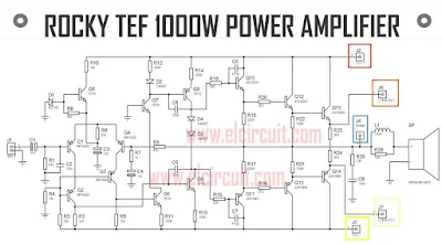
Power Amplifier Circuit Diagram:
Component List:R1= 47K
R2, R5= 1K8/1W
R3= 33K/1W
R4= 15K
R6= 27K
R7= 1K
R8= 47K/1W
R9= 6K8
R10= 10K
R11, R12, R13, R14= 100R/1W
R15, R16 = 22R/1W
R17, R18=220R/5W or 470R/2W x2 Parallel
R19, R20= 2R2/W
R21, R22= 120R/5W or 220R/2W x 2 Parallel
R23, R24= 22R/2W
R25, R26= 10R/5W
C1= 10uF/50V
C2= 120nF
C3, C4= 220uF/80V
C5, C6= 120pF
C7, C8= 470pF
C9= 100nF/275V
D1= Diode Zener 33V
D2,D3,D4= 1N4007
Q1,Q2,Q3,Q4= MPSA92/ 2N5401
Q5,Q6,Q7,Q9= TIP31/ 2SC4793
Q8= TIP32/ 2SA1837
Q10, Q12, Q15= 2SC5200
Q11, Q13, Q14= 2SA1943
L1= 10uH
J1= Input
J2= V+ 45 - 70V DC
J3= V- 45 - 70V DC
J4= Emitter
J6= Base +
J7= Base -
SP= Speaker Output
PCB Layout Design Power Rocky TEF 1000W
PCB Size: 120mm x 80mm
Making PCB Power Amplifier Rocky TEF [VIDEO]
.jpg)


lumayannn....
ReplyDeleteIs it possible to send me better quality PCB, and layout files, also schematic diagram please [email protected]
ReplyDeleteDo you reply to any messages, I have left many and as yet no reply....please reply to your messages
ReplyDeletecan you send me a pdf for this project?? send me the pcb lay out and partslist
ReplyDeleteSir i'll try to make this project because it's very interesting.
ReplyDeletebạn có thể gửi cho mình bản pdf của dự án này. mình rất thích nó và sẽ cố gắng thực hiện nó. mail của mình; [email protected]
ReplyDeleteCan you send me a pdf for this project ?? send me pcb pose and list of parts
ReplyDelete[email protected]
ReplyDeleteHe boss! R9 gak keliru a? kudu ne R9 lead pertama ke Kolektor dan lead kedua sudah sesuai. Mohon di cek lagi.Kalau saya cek PCB nya sudah benar. Penerjemahan ke skema saja yang perlu diperbaiki.Salam kenal dari sesama penggiat elektronika. link https://yohanindrawijaya.com
ReplyDeleteHi boss! its R9 is in the correct position? The resistor should be placed between collector and base of the Q5 transistor. Not between Base and Emitter.I see your PCB and your resistor R9 was correct . Thank you.https://yohanindrawijaya.com
Enter your comment...very nice idea, I like this project
ReplyDelete