2N3055 MJ2955 Booster Transistor Circuit
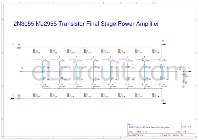
Before , this circuit is boost on Final transistor Power Amplifier 2N3055 MJ2955 , this modif in Final Stage amplifier by adding more 2N3055 and MJ2955 about adding 8 set transistor. Ouput gained to about 500Watt power output. All final transistor circuits are combined in parallel, see circuit diagram below
The addition of transistors you can see in the above schemes combine p2 - p6 correctly with Driver power amplifier. Do not wrong connect, because it can lead to broken transistor. We also completing with pcb board layout making it easy to assemble. Do not Forget to give cooling to the transistor. Place the transitor cooler attached between the pcb and transistors.
Driver Power Amplifier Circuit for 2N3055 and MJ2955
PCB Layout Design 2N3055 MJ2955 Booster Transistor Circuit with Component
PCB Layout Design 2N3055 MJ2955 Booster Transistor Circuit [ PCB Line ]
.jpg)


![PCB Layout Design 2N3055 MJ2955 Booster Transistor Circuit [ PCB Line ] PCB Layout Design 2N3055 MJ2955 Booster Transistor Circuit [ PCB Line ]](https://blogger.googleusercontent.com/img/b/R29vZ2xl/AVvXsEjqIQeGdQPwm6Q1icTla9OB4-51ahu9WFohHdRV3rZh9MwP2mM94pKjrx6AfvaDD6eIMVUkV06cXmG3Chn57vhzb4OlQREy5Qa7718Zj6lvq-_rcZQl-0maOPpfMLRoxD0eYfYBGDtOmVk/s640-rw/Final+Transistor+Booster+2N3055.jpg)
and power supply ???? psu ???
ReplyDeleteit same as the driver supply
ReplyDeleteI m impressed !
ReplyDelete