Super Bass Power Amplifier 2SC2922-2SA1216
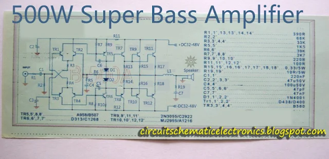
This power amplifier same as Power Amplifier 500W but the difference on the components used ,so will result super bass amplifier. Power amplifier circuit is very nice used for subwoofer applications with powerful bass tones. Power is quite high power amplifier, power power issued about 500 Watt. With sustained by the buffer circuit and the drivers were very fitting for a booster transistor 2SC2922 and 2SA1216 which will emit high power. But if you want to reduce the output power you can use transistor 2N3055 and MJ2955. check on the search engines for the transistor datasheet.
Super Bass Power Amplifier Circuit Diagram
Above is a schematic of the circuit power amplifier super bass. For the power supply voltage, you can supply the voltage 32 volts DC to 48 volts DC.
And I have prepared for assembly pcb layout design. So it will be easier for you to assemble this Super Bass Power Amplifier.
.jpg)


Hi plz can you help me a power amplifier circuit diagram volt 95×2
ReplyDeleteHi plz can you help me a power amplifier circuit diagram volt 95×2
ReplyDeleteyou can search here on high power amplifier. that have voltage supply about it.
DeleteI find a mistake on the PCB layout for the 500W Super Bass Amplifier as you will see,the transistor TR 9 2 N 3055 N TR 11 C 2922 bass pin is marked in the centre but on the transistor middle pin is collector.And also 2 N 3055 is a TO 3 transistor which can not be mounted on your pcb board. Please explain me on [email protected]
ReplyDeleteI find a mistake on the PCB layout for the 500W Super Bass Amplifier as you will see,the transistor TR 9 2 N 3055 N TR 11 C 2922 bass pin is marked in the centre but on the transistor middle pin is collector.And also 2 N 3055 is a TO 3 transistor which can not be mounted on your pcb board. Please explain me on [email protected]
ReplyDeleteIf any personal question, visit contact us page
DeletePdf file sir for this amplifier
ReplyDeletethere is no pdf file
DeleteThank you all.
ReplyDeletePlease I want to know the output frequency since it is not mention here and tell me the exact circuit if it is going to used as 20Hz subwoofer system.
Hi it me again.
ReplyDeleteI mean i want the low pass circuit that will lead the super bass amplifier to 20Hz system
I find a mistake on the PCB layout for the 500W Super Bass Amplifier as you will see,the transistor TR 9 2 N 3055 N TR 11 C 2922 bass pin is marked in the centre but on the transistor middle pin is collector.And also 2 N 3055 is a TO 3 transistor which can not be mounted on your pcb board. Please explain me on [email protected]
ReplyDelete